
Cadence has unveiled a new Chiplet Spec-to-Packaged Parts ecosystem aimed at reducing engineering complexity and accelerating time to market for customers developing chiplets for physical AI, data centre and high-performance computing (HPC) applications.
The ecosystem brings together a broad set of IP and silicon analytics partners, including Arm, Arteris, eMemory, M31 Technology, Silicon Creations and Trilinear Technologies, along with silicon analytics specialist proteanTecs. To further de-risk adoption, Cadence is also collaborating with Samsung Foundry to develop a silicon prototype demonstration of its Physical AI chiplet platform, featuring pre-integrated partner IP on Samsung Foundry’s SF5A process.
Accelerating physical and infrastructure AI innovation
Building on a long-standing collaboration, Cadence and Arm are working closely to accelerate innovation across physical and infrastructure AI use cases. Cadence will leverage the Arm Zena Compute Subsystem (CSS) and other essential IP to enhance its Physical AI chiplet platform and Chiplet Framework.
The resulting solutions are designed to address next-generation edge AI processing requirements for automobiles, robotics and drones, while also supporting standards-based I/O and memory chiplets for data centre, cloud and HPC workloads. According to Cadence, this approach lowers engineering risk, simplifies adoption and enables faster deployment of chiplet-based architectures.
“Cadence’s new chiplet ecosystem represents a significant milestone in chiplet enablement,” said David Glasco, Vice President, Compute Solutions Group, Cadence. “By combining our extensive IP and SoC design expertise with pre-integrated and pre-validated IP from our robust partner ecosystem, Cadence is accelerating the development of chiplet-based solutions and helping customers mitigate risk to quickly realise their chiplet ambitions with greater confidence.”
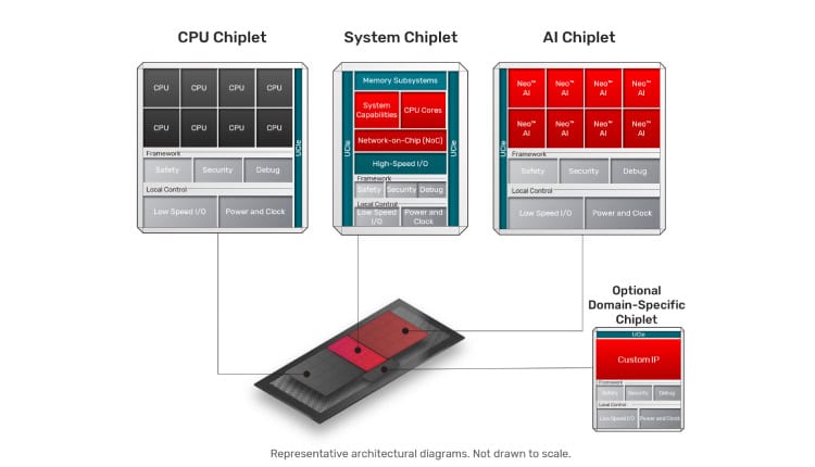
Spec-driven automation and standards compliance
At the core of the initiative is Cadence’s spec-driven automation, which generates chiplet framework architectures by combining Cadence IP with third-party partner IP. These architectures incorporate chiplet management, security and safety features, supported by advanced software and automated EDA flows.
Simulation and verification are enabled through the Cadence Xcelium Logic Simulator and the Cadence Palladium Z3 Enterprise Emulation Platform, while physical design leverages real-time feedback to streamline place-and-route cycles. The architectures are standards-compliant, supporting interoperability across the broader chiplet ecosystem, including adherence to the Arm Chiplet System Architecture and future OCP Foundational Chiplet System Architecture.
Cadence’s Universal Chiplet Interconnect Express (UCIe) IP delivers industry-standard die-to-die connectivity, complemented by a comprehensive protocol IP portfolio supporting advanced interfaces such as LPDDR6/5X, DDR5-MRDIMM, PCI Express 7.0 and HBM4.
With the launch of this partner ecosystem, Cadence is positioning itself to help customers move faster from chiplet specifications to packaged silicon, as multi-die and chiplet-based architectures become central to scaling performance and efficiency in AI and HPC systems.