


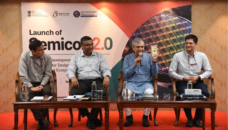

Union Minister for Electronics and Information Technology Ashwini Vaishnaw on Monday outlined the government’s plans for the next phase of India’s semiconductor programme as notifications for all six pillars of the Semicon 2.0 scheme were issued.
The scheme will provide fiscal and infrastructure support across the semiconductor value chain, covering chip design, fabrication, packaging, equipment and materials, research and development, and talent development.
Semicon 2.0 will operate across six pillars: design; machines and materials; setting up more fabs; strengthening the ATMP/OSAT industry; research and development; and talent development.
The design pillar covers semiconductor IPs, chips, system-on-chips and modules for strategic and commercial applications, as well as a deployment-linked incentive for semiconductor IPs, chips and SoCs.
The machines and materials pillar covers the semiconductor manufacturing ecosystem. The fabs pillar includes silicon semiconductor wafer fabs, compound semiconductor, photonics, sensors and discrete semiconductor fabs, as well as display fabs.
The fourth pillar covers semiconductor assembly, testing, marking and packaging facilities, including outsourced semiconductor assembly and test facilities. The fifth focuses on R&D for advanced semiconductor technologies, while the sixth covers talent development.
Addressing the media, Vaishnaw said India had developed 85,000 semiconductor engineers in four years against a target that had originally been set for 10 years. He said the government had now set a target of developing another one lakh engineers.
Vaishnaw also said students from Tier-II and Tier-III cities had designed more than 250 semiconductor chips. He added that semiconductor projects had recorded commercial production within 13 months of groundbreaking in one case, while approvals for multiple projects had been completed within 200, 150 and 90 days.
According to the minister, the semiconductor ecosystem is expected to create 50,000–60,000 direct jobs, while close to 10% of the global semiconductor industry’s market could be in India in the coming years.
Projects supported under Semicon 2.0 will generally have a duration of up to six years, while the scheme will initially remain open for applications for three years.
The India Semiconductor Mission (ISM) will serve as the nodal agency for the scheme, handling applications, technical and financial appraisal, recommendations and implementation oversight. The design and deployment categories may be implemented with assistance from C-DAC.
The Ministry of Electronics and Information Technology will provide budgetary support, with disbursements made through the nodal agency according to approved conditions. A mid-term assessment is scheduled after three years of implementation, or earlier if required, to assess the scheme and consider modifications or continuation.